Electronics design office, IoT expert
Electronic design office with innovative technical solutions
Altyor’s electronics design office was set up in the 90s, and over the past 30 years has launched almost 200 connected projects. In recent years, our expert engineers have developed skills in eco-design, with the aim of designing electronic products with low environmental impact.
")

Multi-protocol, multi-sensor, multi-functionality
Altyor benefits from a broad spectrum of electronic building blocks. Sigfox, LoRa, Wi-Fi, Lifi, Zigbee, EnOcean. These are just a few examples of the radio protocols already implemented by Altyor teams.
In terms of sensors, Altyor is not to be outdone. Accelerometer, gyroscope, magnetometer, UV, VOC…
Our electronic design office implements the sensors according to your needs and the use of your product.
All stages in the design of a finished product
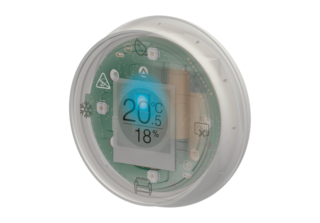
PCB architecture, schematics and routing, firmware. Our RD center studies and designs electronic products (connected or not), integrating all the interfaces of the components created into the architecture. Each functional block is studied in the context of the project as a whole, so as never to forget the interactions between them (energy, EMI, interfaces, radio emissions, etc.).
The industrialisation review ensures that the product defined in the design phase perfectly meets the requirements of industrial production. Mechatronics ensures that the product defined in the design phase fits into the mechanical environment (fixing, dimensions, radio, etc.).
The design phase must also enable the main software functions to be validated, the unit test book to be drawn up, and the test protocol to be drawn up in order to obtain the necessary product certifications.

In order to validate technical solutions, various intermediate mock-ups are produced. These mock-ups will be used to confirm the technological choices made, right up to the prototyping of a functional product, validating the mechanical and electronic aspects.
Do you have a project for us?
Electronics design office with expertise in eco-design
When designing electronic products for our customers, our teams of engineers select components and create products based on 4 criteria: use, durability, optimized consumption and ethics.
Our engineers propose an optimum technical solution tailored to your needs for a sustainable project, because we don’t create single-use products and we design every product so that it lasts over time. To achieve this, our teams make proven technological choices based on our 30 years of experience. They also systematically calculate the MTBF (Mean Time Between Failures) reliability of electronic boards, ensuring the durability of PCBAs. The products are also eco-designed to make them easier to repair, including, where possible, the integration of remote firmware updating, ideally by radio (from the cloud) or nearby (using BLE).
Our expert engineers also work on optimising consumption by choosing low-consumption technologies according to use, by optimising management of operating modes and standby mode (so that the product is only woken up when necessary) or by controlling power supply technologies (leakage current, supply voltage, etc.). And when the product’s use case allows, we use alternative and clean technological solutions for our customers, such as solar, Peltier effect, harvesters, etc., which can offer total or complementary autonomy.
Finally, we check our choice of electronic components against responsible criteria, such as their environmental risks (RoHs and Reach), or their origin outside conflict zones.
Discover all our eco-responsible actions in our Design for Tomorrow policy.


Passionate, committed engineering teams
With over 30 years’ experience behind them, our engineering teams are ready to make proposals throughout your project, right from the design stage.
The flexibility of our RD center enables us to adapt to your product evolutions or modifications during the course of the project.
Come and meet our passionate teams, who will listen to your questions and provide you with personalized answers.
How to design a successful connected object?
Mechanical and electronic design is the first major step in your product journey. It will lead you to the prototyping, industrialization and production phases. In this guide, you’ll discover 18 key points for designing your connected object.
Discover all our references
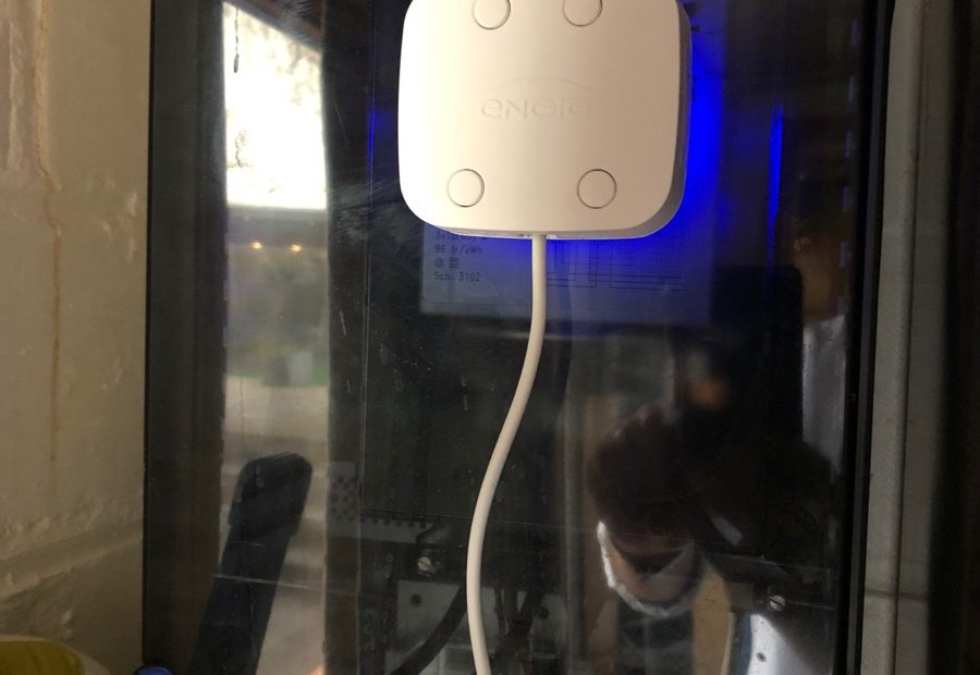
Retrofit of electric meter
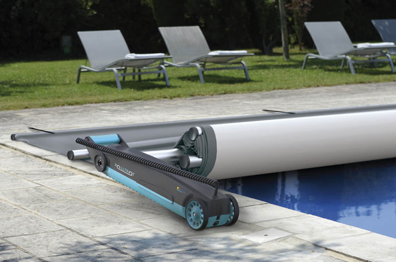
Pool winder
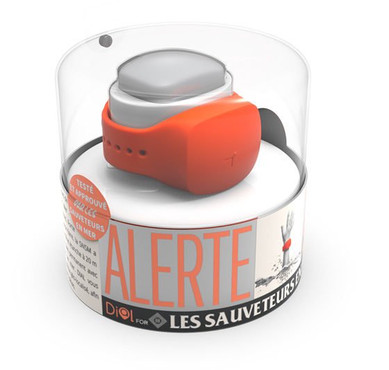
DIAL wristband
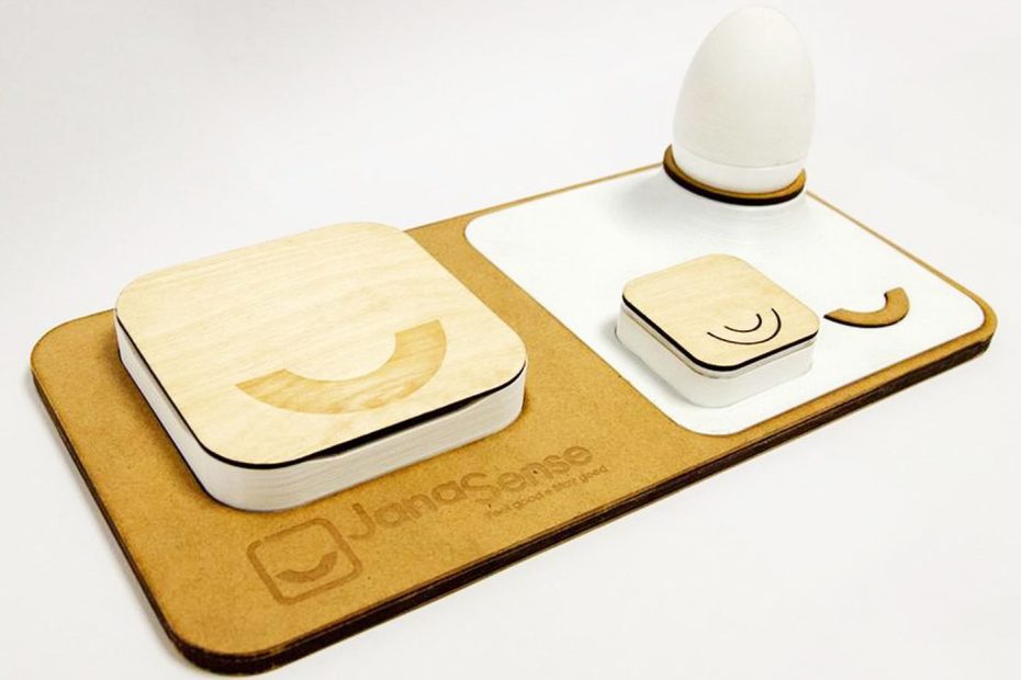
Janabox